Other articles devoted to the construction of this ULF.
Assembly.

Right during the installation, I made a harness or connecting cable. Call it whatever you like.
Since the top and bottom covers cannot be pulled through the pipe, the cable length had to be made redundant. This should allow you to easily reach any element of the circuit without having to unsolder any ends.
The tourniquet was tied with a harsh waxed thread. If there is no such neti, then you can make it from an ordinary one by simply pulling a thread through a candle.
The LED power indicator was glued with hot glue.

Between the microcircuits and the radiator of the final amplifier I placed a gasket made of one layer of medical bandage, generously lubricated with KPT-8 thermal paste. The thickness of the compressed bandage is about 0.1 mm. This gap is quite sufficient even for a voltage of 100 Volts.
Since the entire structure is assembled using one single pin, in order for the pipe to be well fixed in the plugs, I put a rubber ring on the protrusion of each plug (the rings are marked with arrows).
Final assembly of the transformer.
I glued the halves of the magnetic circuit together with epoxy resin and finally assembled the transformer only after the ULF was completely assembled and tested.
If you do not glue the halves of the magnetic circuit together, the transformer will most likely hum. It may hum quieter or louder, but it will be audible.
If you have to break the gluing area, for example, in order to lengthen or shorten the winding, then some plates of the armor core may peel off from the impact. If this happens, it will be very difficult to completely get rid of the buzzing. Therefore, it is better to do gluing at the very end.
To complete the assembly of the transformer, you can wind a layer of electrical cardboard or paper 0.1 mm thick over the coil. It is useful to put data on the windings on paper. If you also wrap a layer of glass or varnish fabric over the paper, the transformer will take on an industrial look.
Setup.
During commissioning, only one error had to be corrected. This error manifested itself in the form of a small hum in the speakers and was caused by incorrect ground routing on the power supply board.

The background appeared due to the fact that a tiny ripple voltage penetrated the input of the voltage stabilizer, and from there into the pre-amplifier.
On the original version of the printed circuit board, the leads of the secondary windings of the transformer going to the case were connected together, which is not correct, since all power grounds should be connected at one point, and not at two.

Initial version of the printed circuit board.

And this is already a modified version. During modification, we had to cut one track, item 1, and add one contact, item 2, to connect the transformer winding that powers the voltage stabilizer.
In addition, another defect has surfaced in the ULF, which has not yet been eliminated. These are clicks when the ULF is turned on and off. The source of the clicks is the volume and tone control unit.

The picture shows a diagram taken at the output of the tone control block. The startup and shutdown of the microcircuit itself occurs very smoothly. Both voltage and sound volume increase within a couple of seconds. But there is a small step in the voltage rise and fall curve, which seems to be caused by some transient processes in the microcircuit. This difference hits the input of the terminals and causes clicks.
I still doubt that Philips has developed such a crooked chip and I blame the specific manufacturer NXP Semiconductors or the batch of chips. First, I’ll try to look for a similar microcircuit from another manufacturer on our radio market.
As I already wrote, an amplifier powered by a bipolar source does not create clicks when turned on and off.
I wouldn’t want to install a loudspeaker shutdown circuit for an amplifier that doesn’t need it.
So, if someone is going to use the TDA1524A, they should pay attention to this circumstance.
Otherwise, the assembly went without any complications.
Ready amplifier.
The pictures show the finished amplifier.

- Cooling gap between the top cover and the radiator.
- Power indicator.
- Network switch.
- Volume.
- Stereo balance.
- HF timbre.
- Bass timbre.
- Phone connection socket.
- Speaker switch.

- Fuse holder.
- Network cable socket.
- Right channel output.
- Line input.
- Left channel output.

- Radiator.
- The only nut that needs to be unscrewed to disassemble the ULF.

- Cooling holes.
- Legs (stoppers from some pharmaceutical bottles).
Measurements.
Ambient temperature – 20ºС.
Mains voltage – 220V.
Sine wave signal – hardware low-frequency generator.
Music cue – Carlos Santana “Jingo: The Santana Collection”.

An oscillogram taken on a ULF load when connected to the input of a low-frequency generator.
Effective power limited by supply voltage ripples – 2x9 Watts.

An oscillogram taken at a load when a music signal is connected to the input.
Peak musical power – 2x18 watts.
Radiator temperature at long work at maximum power, at a frequency of 1 kHz, in power limit mode – 75ºС
The radiator temperature during prolonged music playback at maximum volume limited by supply voltage ripples is 65ºС.
Small details.
The amplifier case turned out to be quite stable. Stability is ensured by the weight of the power transformer and the high coefficient of friction of the rubber feet. When switching the toggle switches, the body does not come off the ground, although it slightly changes position due to the elasticity of the legs.
Of course, it is not possible to cover all cases encountered in repair practice, however, if you follow a certain algorithm, then in the vast majority of cases it is possible to restore the functionality of the device in a very reasonable time. This algorithm was developed by me based on my experience in repairing about fifty different UMZCHs, from the simplest, for a few watts or tens of watts, to concert “monsters” of 1...2 kW per channel, most of which came in for repairwithout circuit diagrams.
The main task of repairing any UMZCH is to localize the failed element, which entails the inoperability of both the entire circuit and the failure of other cascades. Since in electrical engineering there are only 2 types of defects:
- Presence of contact where it should not be;
- Lack of contact where it should be
then the “ultimate task” of repair is to find a broken or torn element. And to do this, find the cascade where it is located. Next is “a matter of technology.” As doctors say: “The correct diagnosis is half the treatment.”
List of equipment and tools necessary (or at least highly desirable) for repairs:
- Screwdrivers, side cutters, pliers, scalpel (knife), tweezers, magnifying glass - i.e., the minimum required set of ordinary installation tools.
- Tester (multimeter).
- Oscilloscope.
- A set of incandescent lamps for various voltages - from 220 V to 12 V (2 pcs.).
- Low-frequency sinusoidal voltage generator (highly desirable).
- Bipolar regulated power supply 15...25(35) V with output current limitation (highly desirable).
- Capacitance and equivalent series resistance meter (ESR) capacitors (highly desirable).
- And finally, the most important tool is a head on your shoulders (required!).
Let's consider this algorithm using the example of repairing a hypothetical transistor UMZCH with bipolar transistors in the output stages (Fig. 1), which is not too primitive, but not very complicated either. This scheme is the most common “classic of the genre”. Functionally, it consists of the following blocks and nodes:
- bipolar power supply (not shown);
- transistor differential input stageVT 2, VT5 with transistor current mirrorVT 1 and VT4 in their collector loads and a stabilizer of their emitter current atVT 3;
- voltage amplifierVT 6 and VT8 in cascode connection, with a load in the form of a current generator onVT 7;
- quiescent current thermal stabilization unit on a transistorVT 9;
- unit for protecting output transistors from overcurrent on transistorsVT 10 and VT 11;
- current amplifier using complementary triplets of transistors connected according to a Darlington circuit in each arm (VT 12 VT 14 VT 16 and VT 13 VT 15 VT 17).
- The first point of any repair is an external inspection of the subject and sniffing it (!). This alone sometimes allows us to at least guess the essence of the defect. If it smells burnt, it means something was clearly burning.
- Checking the presence of mains voltage at the input: the mains fuse has blown, the fastening of the power cord wires in the plug has become loose, there is a break in the power cord, etc. This stage is the most banal in its essence, but at which the repair ends in approximately 10% of cases.
- We are looking for a circuit for the amplifier. In the instructions, on the Internet, from acquaintances, friends, etc. Unfortunately, more and more often in lately– unsuccessfully. If we didn’t find it, we sighed heavily, sprinkled ashes on our heads and started drawing a diagram on the board. You can skip this step. If the result doesn't matter. But it's better not to miss it. It’s boring, long, disgusting, but - “It’s necessary, Fedya, it’s necessary...” ((C) “Operation “Y”...).
- We open the subject and carry out an external inspection of its “gibles”. Use a magnifying glass if necessary. You can see destroyed housings of semi-automatic devices, darkened, charred or destroyed resistors, swollen electrolytic capacitors or electrolyte leaks from them, broken conductors, printed circuit board tracks, etc. If one is found, this is not yet a reason for joy: the destroyed parts may be the result of the failure of some “flea” that is visually intact.
- Checking the power supply.Unsolder the wires coming from the power supply to the circuit (or disconnect the connector, if any). Remove the mains fuse andWe solder a 220 V (60...100 W) lamp to the contacts of its holder. It will limit the current in the primary winding of the transformer, as well as the currents in the secondary windings.
Turn on the amplifier. The lamp should blink (while the filter capacitors are charging) and go out (a faint glow of the filament is allowed). This means that K.Z. There is no mains transformer on the primary winding, and there is no obvious short circuit. in its secondary windings. Using a tester in alternating voltage mode, we measure the voltage on the primary winding of the transformer and on the lamp. Their sum must be equal to the network one. We measure the voltage on the secondary windings. They must be proportional to what is actually measured on the primary winding (relative to the nominal). You can turn off the lamp, replace the fuse and plug the amplifier directly into the network. We repeat the voltage check on the primary and secondary windings. The relationship (proportion) between them should be the same as when measuring with a lamp.
The lamp is constantly burning at full intensity - this means we have a short circuit. in the primary circuit: we check the integrity of the insulation of the wires coming from the network connector, the power switch, the fuse holder. We unsolder one of the leads going to the primary winding of the transformer. The lamp goes out - most likely the primary winding (or interturn short circuit) has failed.
The lamp burns constantly at incomplete intensity - most likely, there is a defect in the secondary windings or in the circuits connected to them. We unsolder one wire going from the secondary windings to the rectifier(s). Don't get confused, Kulibin! So that later there will be no excruciating pain from incorrect soldering back (mark, for example, with pieces of adhesive masking tape). The lamp goes out, which means everything is in order with the transformer. It’s burning - we sigh heavily again and either look for a replacement for it, or rewind it.
6. It was determined that the transformer is in order, and the defect is in the rectifiers or filter capacitors. We test the diodes (it is advisable to unsolder them under one wire going to their terminals, or unsolder them if it is an integral bridge) with a tester in ohmmeter mode at the minimum limit. Digital testers often lie in this mode, so it is advisable to use a pointer device. Personally, I have been using a beeper for a long time (Fig. 2, 3). Diodes (bridge) are broken or broken - we replace them. Whole – “ring” filter capacitors. Before measurement, they must be discharged (!!!) through a 2-watt resistor with a resistance of about 100 Ohms. Otherwise, you may burn the tester. If the capacitor is intact, when it closes, the needle first deflects to the maximum, and then quite slowly (as the capacitor charges) “creeps” to the left. We change the connection of the probes. The arrow first goes off scale to the right (there is a charge left on the capacitor from the previous measurement) and then creeps to the left again. If you have a capacitance and ESR meter, then it is highly advisable to use it. We replace broken or broken capacitors.
 |
 |
7. The rectifiers and capacitors are intact, but is there a voltage stabilizer at the output of the power supply? No problem. Between the output of the rectifier(s) and the input(s) of the stabilizer(s), we turn on the lamp(s) (chain(s) of lamps) to a total voltage close to that indicated on the housing of the filter capacitor. The lamp lights up - there is a defect in the stabilizer (if it is integral), or in the reference voltage generation circuit (if it is on discrete elements), or the capacitor at its output is broken. A broken control transistor is determined by ringing its terminals (unsolder it!).
8. Is everything okay with the power supply (the voltage at its output is symmetrical and nominal)? Let's move on to the most important thing - the amplifier itself. We select a lamp (or strings of lamps) for a total voltage not lower than the nominal voltage from the power supply output and through it (them) we connect the amplifier board. Moreover, preferably to each of the channels separately. Turn it on. Both lamps came on - both arms of the output stages were broken. Only one - one of the shoulders. Although not a fact.
9. The lamps do not light up or only one of them lights up. This means that the output stages are most likely intact. We connect a 10…20 Ohm resistor to the output. Turn it on. The lamps should blink (there are usually also power supply capacitors on the board). We apply a signal from the generator to the input (the gain control is set to maximum). The lamps (both!) lit up. This means that the amplifier amplifies something (although it wheezes, vibrates, etc.) and further repair consists of finding an element that takes it out of mode. More on this below.
10. For further testing, I personally do not use the amplifier’s standard power supply, but use a 2-polar stabilized power supply with a current limit of 0.5 A. If there is none, you can also use the amplifier’s power supply, connected, as indicated, through incandescent lamps. You just need to carefully insulate their bases so as not to accidentally cause a short circuit and be careful not to break the flasks. But an external power supply is better. At the same time, the current consumption is also visible. A well-designed UMZCH allows supply voltage fluctuations within fairly wide limits. We don’t need its super-duper parameters when repairing, just its performance is enough.
11. So, everything is fine with the BP. Let's move on to the amplifier board (Fig. 4). First of all, you need to localize the cascade(s) with broken/broken component(s). For thisextremely preferablyhave an oscilloscope. Without it, the effectiveness of repairs drops significantly. Although you can also do a lot of things with a tester. Almost all measurements are madeno load(at idle). Let us assume that at the output we have a “skew” of the output voltage from several volts to the full supply voltage.
12. First, we turn off the protection unit, for which we unsolder the right terminals of the diodes from the boardVD 6 and VD7 (in my practice it wasthreecase when the cause of inoperability was the failure of this particular unit). We look at the voltage output. If it has returned to normal (there may be a residual imbalance of several millivolts - this is normal), we callVD 6, VD 7 and VT 10, VT11. There may be breaks and breakdownspassive elements. We found a broken element - we replace and restore the connection of the diodes. Is the output zero? Is the output signal (when a signal from the generator is applied to the input) present? The renovation is complete.
Rice. 4.
Has anything changed with the output signal? We leave the diodes disconnected and move on.
13. Unsolder the right terminal of the OOS resistor from the board (R12 together with the right outputC6), as well as left conclusionsR 23 and R24, which we connect with a wire jumper (shown in red in Fig. 4) and through an additional resistor (without numbering, about 10 kOhm) we connect to the common wire. We bridge the collectors with a wire jumper (red color)VT 8 and VT7, excluding capacitor C8 and the thermal stabilization unit for the quiescent current. As a result, the amplifier is separated into two independent units (an input stage with a voltage amplifier and a stage of output repeaters), which must operate independently.
Let's see what we get as a result. Is the voltage imbalance still there? This means that the transistor(s) of the “skewed” shoulder are broken. We unsolder, call, replace. At the same time, we also check passive components (resistors). The most common variant of the defect, however, I must note that very often it isconsequencefailure of some element in the previous cascades (including the protection unit!). Therefore, it is still advisable to complete the following points.
Is there any skew? This means that the output stage is presumably intact. Just in case, we apply a signal from the generator with an amplitude of 3...5 V to point “B” (resistor connectionsR 23 and R24). The output should be a sinusoid with a well-defined “step”, the upper and lower half-waves of which are symmetrical. If they are not symmetrical, it means that one of the transistors of the arm where it is lower has “burnt out” (lost parameters). We solder and call. At the same time, we also check passive components (resistors).
Is there no output signal at all? This means that the power transistors of both arms flew out “through and through”. It's sad, but you'll have to unsolder everything and ring and then replace it.
Breakage of components is also possible. Here you really need to turn on the “8th instrument”. We check, replace...
14. Have you achieved symmetrical repetition at the output (with a step) of the input signal? The output stage has been repaired. Now you need to check the functionality of the quiescent current thermal stabilization unit (transistorVT9). Sometimes there is a violation of the contact of the variable resistor motorR22 with resistive track. If it is connected in the emitter circuit, as shown in the diagram above, nothing bad can happen to the output stage, because at the base connection pointVT 9 to the divider R 20– R 22 R21 the voltage simply increases, it opens slightly more and, accordingly, the voltage drop between its collector and emitter decreases. A pronounced “step” will appear in the idle output.
However (very often), a tuning resistor is placed between the collector and the VT9 base. An extremely foolproof option! Then, when the motor loses contact with the resistive track, the voltage at the base of VT9 decreases, it closes and, accordingly, the voltage drop between its collector and emitter increases, which leads to a sharp increase in the quiescent current of the output transistors, their overheating and, naturally, thermal breakdown. An even more stupid option for performing this cascade is if the VT9 base is connected only to the variable resistor motor. Then, if contact is lost, anything can happen on it, with corresponding consequences for the output stages.
If possible, it is worth rearrangingR22 into the base-emitter circuit. True, in this case the adjustment of the quiescent current will become clearly nonlinear depending on the angle of rotation of the engine, butIMHOThis is not such a big price to pay for reliability. You can simply replace the transistorVT9 to another, with the opposite type of conductivity, if the layout of the tracks on the board allows. This will not affect the operation of the thermal stabilization unit in any way, because he istwo-terminal networkand does not depend on the conductivity type of the transistor.
Testing this cascade is complicated by the fact that, as a rule, connections to the collectorsVT 8 and VT7 are made by printed conductors. You will have to lift the legs of the resistors and make connections with wires (Figure 4 shows wire breaks). Between the buses of positive and negative supply voltages and, accordingly,collector and emitterVT9, resistors of approximately 10 kOhm are turned on (without numbering, shown in red) and the voltage drop across the transistor is measuredVT9 when rotating the trimmer resistor engineR22. Depending on the number of repeater stages, it should vary within approximately 3...5 V (for “triples, as in the diagram) or 2.5... 3.5 V (for “twos”).
15. So we got to the most interesting, but also the most difficult - the differential cascade with a voltage amplifier. They only work together and it is fundamentally impossible to separate them into separate nodes.
We bridge the right terminal of the OOS resistorR12 with collectorsVT 8 and VT 7 (dot " A", which is now his "exit"). We get a “stripped-down” (without output stages) low-power op-amp, which is fully operational at idle (without load). We apply a signal with an amplitude from 0.01 to 1 V to the input and see what happens at the pointA. If we observe an amplified signal of a form symmetrical relative to the ground, without distortion, then this cascade is intact.
16. The signal is sharply reduced in amplitude (low gain) - first of all, check the capacitance of the capacitor(s) C3 (C4, since, to save money, manufacturers very often install only one polar capacitor for a voltage of 50 V or more, hoping that reverse polarity it will still work, which is not the case). When it dries out or breaks down, the gain decreases sharply. If there is no capacitance meter, we simply check by replacing it with a known good one.
The signal is skewed - first of all, check the capacitance of capacitors C5 and C9, which shunt the power buses of the preamplifier section after resistors R17 and R19 (if these RC filters exist at all, since they are often not installed).
The diagram shows two common options for balancing the zero level: with a resistorR 6 or R7 (there may, of course, be others), if the contact of the motor is broken, the output voltage may also be skewed. Check by rotating the engine (although if the contact is “completely broken”, this may not give a result). Then try to bridge their outer terminals with the output of the engine using tweezers.
There is no signal at all - we look to see if it is even present at the input (break in R3 or C1, short circuit in R1, R2, C2, etc.). Just first you need to unsolder the VT2 base, because... the signal on it will be very small and look at the right terminal of resistor R3. Of course, the input circuits may differ greatly from those shown in the figure - include the “8th instrument”. Helps.
17. Naturally, it is not realistic to describe all possible cause-and-effect variants of defects. Therefore, further I will simply outline how to check the nodes and components of this cascade.
Current stabilizersVT 3 and VT7. Breakdowns or breaks are possible in them. The collectors are desoldered from the board and the current between them and the ground is measured. Naturally, you first need to calculate what it should be based on the voltage at their bases and the values of the emitter resistors. (N. B.! In my practice, there was a case of self-excitation of an amplifier due to an excessively large resistor valueR10 supplied by the manufacturer. It helped to adjust its nominal value on a fully working amplifier - without the above-mentioned division into cascades).
You can check the transistor in the same way.VT8: if you jumper the collector-emitter of the transistorVT6, it also stupidly turns into a current generator.
Transistors of the differential stageVT 2 V 5 Tand current mirrorVT 1 VT 4 and also VT6 are checked by checking them after desoldering. It is better to measure the gain (if the tester has such a function). It is advisable to choose ones with the same gain factors.
18. A few words “off the record.” For some reason, in the overwhelming majority of cases, transistors of greater and greater power are installed in each subsequent stage. There is one exception to this dependence: the transistors of the voltage amplification stage (VT 8 and VT 7) are dissipated 3…4 times more power than on the pre-driver VT 12 and VT 23 (!!!). Therefore, if possible, they should be immediately replaced with medium power transistors. A good option would be KT940/KT9115 or similar imported ones.
19. Quite common defects in my practice were non-soldering (“cold” soldering to tracks/“spots” or poor servicing of the leads before soldering) of component legs and broken leads of transistors (especially in a plastic case) directly near the case, which were very difficult to see visually . Shake the transistors, carefully observing their terminals. As a last resort, unsolder and solder again.
If you have checked all the active components, but the defect remains, you need (again, with a heavy sigh), remove at least one leg from the board and check the ratings of the passive components with a tester. There are frequent cases of breaks in permanent resistors without any external manifestations. Non-electrolytic capacitors, as a rule, do not break through/break, but anything can happen...
20. Again, based on repair experience: if darkened/charred resistors are visible on the board, and symmetrically in both arms, it is worth recalculating the power allocated to it. In the Zhytomyr amplifier “Dominator”, the manufacturer installed 0.25 W resistors in one of the stages, which regularly burned (there were 3 repairs before me). When I calculated their required power, I almost fell out of my chair: it turned out that they should dissipate 3 (three!) watts...
21. Finally, everything worked... We restore all the “broken” connections. The advice seems to be the most banal, but how many times is it forgotten!!! We restore in the reverse order and after each connection we check the amplifier for functionality. Often, a step-by-step check seemed to show that everything was working properly, but after the connections were restored, the defect “crept out” again. Lastly, we solder the diodes of the current protection cascade.
22. Set the quiescent current. Between the power supply and the amplifier board we turn on (if they were turned off earlier) a “garland” of incandescent lamps at the corresponding total voltage. We connect an equivalent load (4 or 8 ohm resistor) to the UMZCH output. We set the engine of the trimming resistor R 22 to the lower position according to the diagram and apply a signal to the input from a generator with a frequency of 10...20 kHz (!!!) of such an amplitude that the output signal is no more than 0.5...1 V. At such a level and frequency There is a clearly visible “step” in the signal, which is difficult to notice at a large signal and low frequency. By rotating the R22 engine we achieve its elimination. In this case, the filaments of the lamps should glow a little. You can also monitor the current with an ammeter by connecting it in parallel with each garland of lamps. Don’t be surprised if it differs noticeably (but no more than 1.5…2 times more) from what is indicated in the setup recommendations - after all, what’s important to us is not “following the recommendations,” but the sound quality! As a rule, in “recommendations” the quiescent current is significantly overestimated in order to guarantee the achievement of the planned parameters (“at worst”). We bridge the “garlands” with a jumper, increase the output signal level to a level of 0.7 from the maximum (when the amplitude limitation of the output signal begins) and let the amplifier warm up for 20...30 minutes. This mode is the most difficult for the transistors of the output stage - the maximum power is dissipated on them. If the “step” does not appear (at a low signal level), and the quiescent current has increased no more than 2 times, we consider the setup complete, otherwise we remove the “step” again (as indicated above).
23. We remove all temporary connections (don’t forget!!!), assemble the amplifier completely, close the case and pour a glass, which we drink with a feeling of deep satisfaction for the work done. Otherwise it won't work!
Of course, this article does not describe the nuances of repairing amplifiers with “exotic” stages, with an op-amp at the input, with output transistors connected with an OE, with “double-deck” output stages, and much more...
That's why TO BE CONTINUED…
A correctly assembled ULF when the transistor modes correspond to the diagrams (see Fig. 63 - 68) and table. 3 should immediately work normally when a signal from a sound generator (SG) is applied to the input. Therefore, the process of setting up and adjusting a low-frequency amplifier comes down to checking the sensitivity, the magnitude of nonlinear distortion and frequency response, as well as eliminating the faults identified during this process, due to which one or another parameter will not correspond to the standard.
Before starting measurements, it is advisable to check the current consumption of the low-frequency amplifier in the absence of a signal. To do this, all transistors up to the ULF block are removed (soldered off) and the current is measured. For example, for radio receivers of the "Speedola" type, this current is 6 - 8 mA. If the measured current exceeds this value, it is necessary to replace the transistor of the first ULF stage with a triode with a higher gain.
Next, the SG is connected to the input of the bass amplifier. For receivers of the "Spidola" type, the generator is connected to pin 10 of the IF-LF board (see Fig. 2) or lobe 1 of the R30 potentiometer (see Fig. 21), and the ground terminal of the CG is connected to pin 7 of the IF-LF board or lobe 3 potentiometer R30. For other receivers, the sound generator is connected to the corresponding terminals of the “tape recorder” connector (W).
A tube voltmeter (LV), an oscilloscope and a nonlinear distortion meter (NID) are connected to the output of the receiver (Fig. 69) parallel to the voice coil of the loudspeaker. For all receivers, these devices are connected to the external speaker jacks on the block external connections or to the corresponding contacts of the “tape recorder” connector (W).
Below we discuss the procedure for setting up and testing ULF receivers such as “Spidola”, “VEF-12”, “VEF-201”, and “VEF-202”. Data on setting up and testing ULF radio receivers of the “Ocean” type are summarized in table. 4; "Spidola-207" and "Spidola-230" - in table. 5. Setting up the Meridian-202 receiver, which has significant differences in electrical diagram, is described in § 18.
To test the sensitivity of ULF radio receivers such as "Spidola", "VEF-12", "VEF-201" and "VEF-202", the frequency of the sound generator is set to 1000 Hz and the output voltage is no more than 15. The volume control (RG) is set to the maximum volume position, and the tone control (“VEF-12”, “VEF-201” in “VEF-202”) is set to the wide band position (raising high frequencies). In this case, a sound with a frequency of 1000 Hz will be heard in the loudspeaker, and the output voltmeter will show the voltage value of this frequency. The SG output regulator sets the voltage at which the output will be 0.56 V (1.1 V for “VEF-12”, “VEF-201” and “VEF-202”). This voltage corresponds to the rated output power. The voltage at the output of the MG will be the sensitivity of the LF path.
Rice. 69. Block diagram of setting up and testing ULF receivers 1,2 - input of the ULF block; 3,4 - external speaker socket or “tape recorder” connector (III)
In parallel with the sensitivity check, nonlinear distortions of the low-frequency amplification path are checked using the INI readings. The coefficient of nonlinear distortion should not exceed the values indicated in table. 2, and the image of the sinusoid on the oscilloscope screen should be without distortion. In case of severe distortion, it is necessary to replace transistors T9 and T10. Increased nonlinear distortions can also be caused by incorrect wiring of the terminals of the matching and output transformers (the signal from the VLF output is in phase with the input signal). In this case, it is necessary to transfer the ends of the secondary winding of the transformers. In addition, the reason may be the incorrectly selected capacitance of the capacitor C80 and C81 ("Spidola"), C77 and C76 ("VEF-12", "VEF-201", "VEF-202") and the resistance of the resistor R36 ("Spidola" ), R42 (“VEF-12”, “VEF-201”, “VEF-202”).

Table 4

Table 4

Table 5
To check the frequency response of the ULF, the frequency of the sound generator is set to 1000 Hz. The volume control at the ULF output sets the voltage to 0.56 V ("Spidola"), 1.1 V ("VEF-12", "VEF-201", "VEF-202") and then the position of the RG does not change. The input voltage (mx) should not exceed 12 mV ("Spidola"), 10 mV ("VEF-12", "VEF-201", "VEF-202"). Then a signal with a frequency of first 200 Hz and then 4000 Hz (playback band) is supplied to the ULF input, and in both cases the voltage u2t is set by the regulator of the output of the generator, which corresponds to the output voltage of 0.56 V (1.1 V). The unevenness of the frequency response N is determined from the ratio N = 20 lg (u2/u1) and should not exceed the standards specified in table. 2. Correction of the frequency response can be carried out by selecting the capacitance of the capacitor C78 ("Spidola"), C73 ("VEF-12", "VEF-201", "VEF-202").

Rice. 70. Block diagram of measuring the input resistance of ULF receivers 1,2 - ULF input; Hin - resistance between points 1 and 2
Sometimes it is useful to know the input impedance of a low-frequency amplifier. For this, a circuit is assembled in accordance with Fig. 70.
The volume control is set to the maximum volume position. From the SG, a signal with a frequency of 1000 Hz is supplied to the base of the first transistor of the low-frequency amplifier through a resistor R1 (2 - 3 kohms) of such a value that the output voltage is 0.56 V ("Spidola") and 1.1 V ("VEF-12" , "VEF-201", "VEF-202"). In this case, the lamp voltmeter (LV1) at the output of the SG will show the voltage value ut, and LV2 - u2 (VLF input). Knowing the value of R1 and the voltages u2 and u1, you can calculate the input resistance of the amplifier (RBX) using the formula:
Rin = u2 R1/uR1 = u2/(u1-u2) R1,
where uR1 == u1 - u2.
The value of resistor R1 is selected so that it is 2 and 2.
If at the ULF output a voltage corresponding to the rated output power can be obtained at very low input voltages, then this will indicate that the amplifier is close to self-excitation. The reasons for this phenomenon may be positive feedback instead of negative, an open circuit in the feedback circuit, or incorrect wiring of the matching (output) transformer terminals. This mode is characterized by a very high nonlinear distortion coefficient and large uneven frequency response.
After completing the ULF adjustment, you need to turn on the supply voltage and check by ear the operation of the low-frequency amplifier at all positions of the volume control. At the position of the RG, corresponding to the minimum volume, there should be no signal at the output of the receiver, and at maximum volume and a ULF signal from the RG with a frequency of 1000 Hz and a value of 15 - 25 mV is supplied to the input, the shape of the output voltage should be undistorted and without kinks, shining brightly points, etc.

Rice. 2. Wiring diagram of the IF-LF board of the “Spidola”, “VEF-Spidola” and “VEF-Spidola-10” radio receivers. Resistor R42 is installed on the foil side

Rice. 6. Wiring diagram of the IF-LF board of the VEF-12, VEF-201 and VEF-202 radio receivers. Resistors R10, R22 and R47 are installed on the foil side

Rice. 10. Wiring diagrams of range strips 25 m - P1, 31 m - P2, 41 m - PZ, 49 m - P4 (a), - 50 - 75 g - P5 (b); SV - P6(v) and DV - P7(g) of the Ocean radio receiver. On the bands of 25 m (P1) and 31 m (P2) there is no choke (Dr), its connection points are short-circuited with a jumper
Rice. 11. Wiring diagram of the board of the VHF radio receiver “Ocean”

Rice. 12. Wiring diagram of the HF-IF board of the Ocean radio receiver. The diagram does not show the screens of transistors TZ, T4, T5, T8 and T9 and the position of the moving knives of switch B1. Points 20 and 21 of the board are connected by a jumper
Rice. 13. Wiring diagram of the ULF radio receiver board "Ocean"

Rice. 15. Wiring diagrams of the strips for ranges 2o m - P1, 31 m - P2, Im - PZ, 49 m - - P4(a); 50 - 75 m - 115(6) of the Ocean-203 radio receiver. On the bands of 25 m (III) and 31 l (P2) ranges there is no choke (Dr), its connection points are short-circuited with a jumper

Rice. 16. Wiring diagram of the board of the VHF radio receiver “Ocean-203”
Rice. 17. Wiring diagram of the HF-G1Ch board of the Ocean-203 radio receiver. The diagram does not show the screens of transistors TZ, T4, T5, T8 and T9 and the position of the movable knives of switch B1
Rice. 18. Wiring diagram of the ULF radio receiver board "Ocean-203"

Rice. 20. Wiring diagram - boards of the VHF radio receiver "Ocean-205"
Rice. 21. Wiring diagram of the ULF radio receiver board "Ocean-205"
Rice. 22. Wiring diagram of the rectifier board of the Ocean-205 radio receiver

Rice. 23. Wiring diagram of the board of switches B2 - B5 of the Ocean-205 radio receiver
Rice. 24. Wiring diagrams of range strips 25 m - P1, 31 g-P2, 41 m - PZ, 49 m - P4(a); 50-75 m - P5(6j; CB - P6(c); DV - P7(g) radio receiver "Ocean-205" On the strips of the ranges 41 m (LZ) and 49 L1 (U4) instead of a jumper between points A and B is installed throttle (Dr)

Rice. 25. Section of the wiring diagram of the HF-IF board of the Ocean-205 radio receiver with a modified print
Rice. 27. Wiring diagrams of strips for ranges 25 f - P1, 31 M - .P2, 41 m - PZ, 49 m~P4(a); 52-75 m - 115(6); SV - P6(c); DV - P7(g) radio receivers "Spidola-207" and "Spidola-230"

Rice. 28. Wiring diagram of the IF-LF board of the Spidola-207 radio receiver. The screens of transistors TZ - T7 are shown conditionally. The positions of the moving knives of switches B1 - B5 are not shown

Before adjusting the ULF, you should touch with tweezers an ungrounded socket for connecting a pickup or directly to the control grid of the first amplifier tube. If the amplifier is running, there will be a strong hum in the speaker. The volume control should be in the position corresponding to the maximum volume.
It is also necessary to connect the devices correctly. First of all, connect all the terminals to be grounded. The terminals of the devices located on the input side are connected to the Ground terminal of the amplifier's input, and the corresponding terminals of the output devices are connected to the Ground terminal of the amplifier's output. Then the ground terminals of the input and output of the amplifier are connected with a jumper. The sound generator is connected to the amplifier input using a shielded wire; the shield is reliably grounded.
Then the receiver is turned on to play the record, and the volume control is set to the maximum gain position. If the receiver has a tone control, then the test is carried out at various positions of this control. At any position of the tone controls and maximum volume, the amplifier should not be excited. Excitation is detected when an intermittent sound or whistles of various tones appear in the loudspeaker, as well as by readings from measuring equipment.
In addition to self-excitation, an alternating current hum may appear in the amplifier. The presence of background is also checked when there is no signal at the amplifier input.
Then they begin to check the operation of the amplifier in the presence of a signal at the input. As an example, consider the procedure for checking the ULF of the Sirius-309 industrial receiver.
The output hose of a GZ-33 type sound generator or a similar device is connected to the block for connecting a tape recorder. An output meter of type VZ-2A is connected in parallel to the secondary winding of the output transformer. The radio is turned on to play a record. The volume control and tone control should be in the position of maximum gain and maximum bandwidth. The generator is set to a signal with a frequency of 1000 Hz and an output voltage level at which the voltage on the VZ-2A output meter will be 0.8V, which corresponds to the rated output power. The output voltage of the sound generator is the sensitivity of the ULF and should be no worse than 80 mV for a given radio. For receivers of other brands, with an output voltage of the sound generator of 0.2...0.25V, the amplifier must deliver power close to the rated one to the load.
After this, check the frequency response of the amplifier and the operation of the tone and volume controls. A signal equal to 0.25 V with a frequency of 1000 Hz is supplied to the ULF input from the generator. The tone control is set to the position corresponding to the cutoff of higher sound frequencies. Using the volume control on the output meter, set the voltage to 0.8 V. Then, without changing the voltage, set the frequency to 5000 Hz on the sound generator. In this case, the output voltage on the output meter should decrease to 0.4 V.
To check the operation of the volume control, it is necessary to apply to the input of the radio from a generator type G4-102 a voltage modulated in amplitude by a voltage of 1000 Hz with a modulation depth of 30%, at which the output meter will show a voltage of 2.5 V. The volume control should be in the position maximum volume. The volume control is then set to the minimum volume position and the output meter reading is noted. The ratio of the voltage (at the receiver output) corresponding to the rated output power to the voltage corresponding to the minimum volume position of the volume control (in decibels) must be at least 40 dB.
When checking the frequency response and the operation of the tone and volume controls, you must ensure that the voltage at the output of the sound generator corresponds to 250 mV. The limits for measuring the output voltage when checking the frequency response and adjusting the tone and volume in receivers of other brands should be indicated in the repair instructions in the form of a table.
The method for testing ULF with a single-cycle output stage was discussed above. In high-quality ULF receivers of the first and highest classes and transistor receivers, the final stages are assembled using push-pull circuits.
The setup of push-pull output stages begins with the phase inversion stage. When adjusting this cascade, the same output voltage values are set, shifted in phase by 180°. To do this, select the resistance values of the resistors in the collector and emitter circuits. Transistors used in a push-pull power amplifier circuit must have the same parameters. It’s good if the transistors’ collector currents and current gain differ by no more than ±10%. If the transistors are not identical in parameters, then the bias voltage must be adjusted using resistors connected in the base circuits. The condition for the normal operation of a push-pull final stage is the symmetry of its arms in both direct and alternating current.
If you need to check the polarity of the connection of the feedback circuit, a signal with a frequency of 1000 Hz is supplied to the ULF input from the sound generator, such a value at which the output voltage would be approximately half the nominal one. Then short-circuit the resistor from which the feedback voltage is removed and observe the readings of the output voltage meter. If at the same time the output meter readings increase, then the polarity of the feedback is negative (correct), and if they decrease, it is positive. To change the polarity, it is necessary to swap the ends of the secondary winding of the output transformer.
The final stage of adjusting the amplifier is checking all its quality indicators: a) measuring the output power; b) taking the frequency response; c) measurement of harmonic distortion coefficient; d) checking the background level.
Figure 1 Circuit of the LANZAR power amplifier entirely based on bipolar transistors.
INCREASE

Figure 2 LANZAR power amplifier circuit using field effect transistors in the penultimate cascade.
INCREASE

Figure 3 Circuit of the LANZAR power amplifier from the MS-8 simulator. INCREASE
|
LIST OF ELEMENTS INSTALLED IN THE LANZAR AMPLIFIER |
|
|
FOR BIPOLAR OPTION |
FOR THE OPTION WITH FIELDS |
| C3,C2 = 2 x 22µ0 C4 = 1 x 470p C6,C7 = 2 x 470µ0 x 25V C5,C8 = 2 x 0µ33 C11,C9 = 2 x 47µ0 C12,C13,C18 = 3 x 47p C15,C17,C1,C10 = 4 x 1µ0 C21 = 1 x 0µ15 C19,C20 = 2 x 470µ0 x 100V C14,C16 = 2 x 220µ0 x 100V R1 = 1 x 27k VD1,VD2 = 2 x 15V VT2,VT4 = 2 x 2N5401 |
C3,C2 = 2 x 22µ0 C4 = 1 x 470p C6,C7 = 2 x 470µ0 x 25V C5,C8 = 2 x 0µ33 C11,C10 = 2 x 47µ0 C12,C13,C18 = 3 x 47p C15,C17,C1,C9 = 4 x 1µ0 C21 = 1 x 0µ15 C19,C20 = 2 x 470µ0 x 100V C14,C16 = 2 x 220µ0 x 100V R1 = 1 x 27k VD1,VD2 = 2 x 15V VT8 = 1 x IRF640 |
For example, let's take the supply voltage equal to ±60 V. If the installation is done correctly and there are no faulty parts, then we get the voltage map shown in Figure 7. The currents flowing through the elements of the power amplifier are shown in Figure 8. The power dissipation of each element is shown in Figure 9 (about 990 mW is dissipated on transistors VT5, VT6, therefore the TO-126 case requires a heat sink).

Figure 7. LANZAR power amplifier voltage map ENLARGE

Figure 8. Power amplifier current map ENLARGE

Figure 9. Amplifier power dissipation map ENLARGE
A few words about details and installation:
First of all, you should pay attention to the correct installation of parts, since the circuit is symmetrical, errors are quite common. Figure 10 shows the arrangement of parts. Regulation of the quiescent current (current flowing through the terminal transistors when the input is closed to a common wire and compensating the current-voltage characteristic of the transistors) is carried out by resistor X1. When turned on for the first time, the resistor slider should be in the highest position according to the diagram, i.e. have maximum resistance.
The quiescent current should be 30...60 mA. There is no thought to setting it higher - there are no noticeable changes in either instruments or audibly. To set the quiescent current, the voltage is measured on any of the emitter resistors of the final stage and set in accordance with the table:
|
VOLTAGE AT THE TERMINALS OF THE EMITTER RESISTOR, V |
TOO SMALL STOP CURRENT, POSSIBLE "STEP" DISTORTION NORMAL REST CURRENT, THE STILL CURRENT IS HIGH - EXCESSIVE HEATING, IF THIS IS NOT AN ATTEMPT TO CREATE CLASS "A", THEN THIS IS AN EMERGENCY CURRENT. | |||||
|
REST CURRENT OF ONE PAIR OF TERMINAL TRANSISTORS, mA |
||||||
|
|
|
|
||||
|
|
|
|
||||

Figure 10 Location of parts on the power amplifier board. The places where installation errors most often occur are shown.
The question was raised about the advisability of using ceramic resistors in the emitter circuits of terminal transistors. You can also use MLT-2, two of each, connected in parallel with a nominal value of 0.47...0.68 Ohm. However, the distortion introduced by ceramic resistors is too small, but the fact that they are breakable - when overloaded they break, i.e. their resistance becomes infinite, which quite often leads to the salvation of the final transistors in critical situations.
The radiator area depends on the cooling conditions; Figure 11 shows one of the options, it is necessary to attach power transistors to the heat sink through insulating gaskets
. It is better to use mica, since it has a fairly low thermal resistance. One of the options for mounting transistors is shown in Figure 12.

Figure 11 One of the radiator options for a power of 300 W, subject to good ventilation

Figure 12 One of the options for attaching power amplifier transistors to a radiator.
Insulating gaskets must be used.
Before installing power transistors, as well as in case of suspected breakdown, the power transistors are checked with a tester. The limit on the tester is set to test diodes (Figure 13).

Figure 13 Checking the amplifier's final transistors before installation and in case of suspected breakdown of the transistors after critical situations.
Is it worth selecting transistors according to the code? gain? There are quite a lot of disputes on this topic and the idea of selecting elements dates back to the late seventies, when the quality of the element base left much to be desired. Today, the manufacturer guarantees a spread of parameters between transistors of the same batch of no more than 2%, which in itself indicates the good quality of the elements. In addition, given that the terminal transistors 2SA1943 - 2SC5200 are firmly established in audio engineering, the manufacturer began producing paired transistors, i.e. transistors of both direct and reverse conduction already have the same parameters, i.e. the difference is no more than 2% (Figure 14). Unfortunately, such pairs are not always found on sale, however, we have had the opportunity to buy “twins” several times. However, even having sorted out the coffee code. gain between forward and reverse transistors, you just need to make sure that transistors of the same structure are of the same batch, since they are connected in parallel and the spread in h21 can cause an overload of one of the transistors (which has this parameter higher) and, as a result, overheating and failure building. Well, the spread between the transistors for the positive and negative half-waves is fully compensated by the negative feedback.
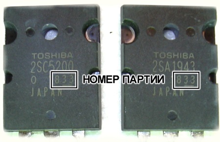
Figure 14 Transistors of different structures, but from the same batch.
The same applies to differential stage transistors - if they are of the same batch, i.e. purchased at the same time in one place, then the chance that the difference in parameters will be more than 5% is VERY small. Personally, we prefer the 2N5551 - 2N5401 transistors from FAIRCHALD, however, the ST also sounds quite decent.
However, this amplifier is also assembled using domestic components. This is quite realistic, but let’s make allowance for the fact that the parameters of the KT817 purchased and those found on the shelves in your workshop, purchased back in the 90s, will differ quite significantly. Therefore, here it is better to use the h21 meter available in almost all digital test rooms. True, this gadget in the tester shows the truth only for low-power transistors. Using it to select transistors for the final stage will not be entirely correct, since h21 also depends on the current flowing. This is why separate testing stands are already being made to reject power transistors. from the adjustable collector current of the transistor being tested (Figure 15). The calibration of a permanent device for rejecting transistors is carried out in such a way that the microammeter at a collector current of 1 A deviates by half the scale, and at a current of 2 A - completely. When assembling an amplifier, you don’t have to make a stand for yourself; two multimeters with a current measurement limit of at least 5 A are enough.
To carry out rejection, you should take any transistor from the rejected batch and set the collector current with a variable resistor to 0.4...0.6 A for transistors of the penultimate stage and 1...1.3 A for transistors of the final stage. Well, then everything is simple - transistors are connected to the terminals and, according to the readings of the ammeter connected to the collector, transistors with the same readings are selected, not forgetting to look at the readings of the ammeter in the base circuit - they should also be similar. A spread of 5% is quite acceptable for dial indicators You can make “green corridor” marks on the scale during calibration. It should be noted that such currents do not cause poor heating of the transistor crystal, and given the fact that it is without a heat sink, the duration of measurements should not be extended over time - the SB1 button should not be held pressed for more than 1...1.5 seconds. Such screening will first of all allow you to select transistors with a really similar gain factor, and checking powerful transistors with a digital multimeter is only a check to ease the conscience - in microcurrent mode, powerful transistors have a gain factor of more than 500, and even a small spread when checking with a multimeter in real current modes can turn out to be huge . In other words, when checking the gain coefficient of a powerful transistor, the multimeter reading is nothing more than an abstract value that has nothing in common with the gain coefficient of the transistor, at least 0.5 A flows through the collector-emitter junction.

Figure 15 Rejection of powerful transistors based on gain.
Feed-through capacitors C1-C3, C9-C11 do not have a completely typical connection, compared to factory analogues of amplifiers. This is due to the fact that with this connection, the result is not a polar capacitor of a rather large capacity, but the use of a 1 µF film capacitor compensates for the not entirely correct operation of electrolytes at high frequencies. In other words, this implementation made it possible to obtain a more pleasant amplifier sound, compared to one electrolyte or one film capacitor.
In older versions of Lanzar, instead of diodes VD3, VD4, 10 Ohm resistors were used. Changing the element base allowed for slightly improved performance at signal peaks. For a more detailed look at this issue, let's look at Figure 3.
The circuit does not model an ideal power source, but one closer to a real one, which has its own resistance (R30, R31). When playing a sinusoidal signal, the voltage on the power buses will have the form shown in Figure 16. V in this case The capacitance of the power filter capacitors is 4700 uF, which is somewhat small. For normal operation of the amplifier, the capacitance of the power capacitors must be at least 10,000 µF per channel, more is possible, but a significant difference is no longer noticeable. But let's return to Figure 16. The blue line shows the voltage directly at the collectors of the final stage transistors, and the red line shows the supply voltage of the voltage amplifier in the case of using resistors instead of VD3, VD4. As can be seen from the figure, the supply voltage of the final stage has dropped from 60 V and is located between 58.3 V in the pause and 55.7 V at the peak of the sinusoidal signal. Due to the fact that capacitor C14 is not only charged through the decoupling diode, but also discharged at signal peaks, the amplifier supply voltage takes the form of a red line in Figure 16 and ranges from 56 V to 57.5 V, i.e. has a swing of about 1.5 IN.

Figure 16 voltage waveform when using decoupling resistors.

Figure 17 Shape of supply voltages on the final transistors and voltage amplifier
By replacing the resistors with diodes VD3 and VD4, we obtain the voltages shown in Figure 17. As can be seen from the figure, the ripple amplitude on the collectors of the terminal transistors has remained almost unchanged, but the supply voltage of the voltage amplifier has taken on a completely different form. First of all, the amplitude decreased from 1.5 V to 1 V, and also at the moment when the peak of the signal passes, the supply voltage of the UA sags only to half the amplitude, i.e. by approximately 0.5 V, while when using a resistor, the voltage at the peak of the signal sags by 1.2 V. In other words, by simply replacing resistors with diodes, it was possible to reduce the power ripple in the voltage amplifier by more than 2 times.
However, these are theoretical calculations. In practice, this replacement allows you to get a “free” 4-5 watts, since the amplifier operates at a higher output voltage and reduces distortion at signal peaks.
After assembling the amplifier and adjusting the quiescent current, you should make sure that there is no constant voltage at the output of the power amplifier. If it is higher than 0.1 V, then this clearly requires adjustment of the operating modes of the amplifier. In this case, the most in a simple way is the selection of the “supporting” resistor R1. For clarity, we present several options for this rating and show the DC voltage measurements at the output of the amplifier in Figure 18.

Figure 18 Change in DC voltage at the amplifier output depending on the value of R1
Despite the fact that on the simulator the optimal constant voltage was obtained only with R1 equal to 8.2 kOhm, in real amplifiers this rating is 15 kOhm...27 kOhm, depending on which manufacturer the differential stage transistors VT1-VT4 are used.
Perhaps it’s worth saying a few words about the differences between power amplifiers using bipolar transistors and those using field devices in the penultimate stage. First of all, when using field-effect transistors, the output stage of the voltage amplifier is VERY heavily unloaded, since the gates of field-effect transistors have practically no active resistance - only the gate capacitance is a load. In this embodiment, the amplifier circuitry begins to step on the heels of class A amplifiers, since over the entire output power range the current flowing through the output stage of the voltage amplifier remains almost unchanged. The increase in the quiescent current of the penultimate stage operating on the floating load R18 and the base of the emitter followers of powerful transistors also varies within small limits, which ultimately led to a rather noticeable decrease in THD. However, there is also a fly in the ointment in this barrel of honey - the efficiency of the amplifier has decreased and the output power of the amplifier has decreased, due to the need to apply a voltage of more than 4 V to the field gates to open them (for a bipolar transistor this parameter is 0.6...0.7 V ). Figure 19 shows the peak of the sinusoidal signal of an amplifier made on bipolar transistors (blue line) and field-field switches (red line) at the maximum amplitude of the output signal.

Figure 19 Change in the amplitude of the output signal when using different elements in the amplifier.
In other words, reducing THD by replacing field-effect transistors leads to a “shortage” of about 30 W, and a decrease in the THD level by about 2 times, so it’s up to each individual to decide what to set.
It should also be remembered that the THD level also depends on the amplifier’s own gain. In this amplifier The gain coefficient depends on the values of resistors R25 and R13
(at the nominal values used, the gain is almost 27 dB). Calculate Gain coefficient in dB can be obtained using the formula Ku =20 lg R25 / (R13 +1), where R13 and R25 are the resistance in Ohms, 20 is the multiplier, lg is the decimal logarithm. If it is necessary to calculate the gain coefficient in times, then the formula takes the form Ku = R25 / (R13 + 1). This calculation is sometimes necessary when making a pre-amplifier and calculating the amplitude of the output signal in volts in order to prevent the power amplifier from operating in hard clipping mode.
Reducing your own coffee rate. gain up to 21 dB (R13 = 910 Ohm) leads to a decrease in the THD level by approximately 1.7 times at the same output signal amplitude (the input voltage amplitude is increased).
Well, now a few words about the most popular mistakes when assembling an amplifier yourself.
One of the most popular mistakes is installation of 15 V zener diodes with incorrect polarity, i.e. These elements do not operate in voltage stabilization mode, but like ordinary diodes. As a rule, such an error causes a constant voltage to appear at the output, and the polarity can be either positive or negative (usually negative). The voltage value is based between 15 and 30 V. In this case, not a single element heats up. Figure 20 shows the voltage map for incorrect installation of zener diodes, which was produced by the simulator. Invalid elements are highlighted in green.

Figure 20 Voltage map of a power amplifier with improperly soldered zener diodes.
The next popular mistake is mounting transistors upside down, i.e. when the collector and emitter are confused. In this case, there is also constant tension and the absence of any signs of life. True, switching the transistors of the differential cascade back on can lead to their failure, but then depending on your luck. The voltage map for an “inverted” connection is shown in Figure 21.

Figure 21 Voltage map when the differential cascade transistors are turned on “inverted”.
Quite often transistors 2N5551 and 2N5401 are confused, and the emitter and collector can also be confused. Figure 22 shows the voltage map of the amplifier with the “correct” installation of interchanged transistors, and Figure 23 shows the transistors not only interchanged, but also upside down.

Figure 22 The differential cascade transistors are reversed.

Figure 23 The transistors of the differential stage are reversed, and the collector and emitter are reversed.
If the transistors are swapped, and the emitter-collector is soldered correctly, then a small constant voltage is observed at the output of the amplifier, the quiescent current of the window transistors is regulated, but the sound is either completely absent or at the level “it seems to be playing.” Before installing transistors sealed in this way on the board, they should be checked for functionality. If the transistors are swapped, and even the emitter-collector places are swapped, then the situation is already quite critical, since in this embodiment, for the transistors of the differential stage, the polarity of the applied voltage is correct, but the operating modes are violated. In this option, there is strong heating of the terminal transistors (the current flowing through them is 2-4 A), a small constant voltage at the output and a barely audible sound.
Confusing the pinout of the transistors of the last stage of the voltage amplifier is quite problematic when using transistors in the TO-220 package, but transistors in the TO-126 package are often soldered upside down, swapping the collector and emitter. In this option, there is a highly distorted output signal, poor regulation of the quiescent current, and lack of heating of the transistors of the last stage of the voltage amplifier. A more detailed voltage map for this power amplifier mounting option is shown in Figure 24.

Figure 24 The transistors of the last stage of the voltage amplifier are soldered upside down.
Sometimes the transistors of the last stage of the voltage amplifier are confused. In this case, there is a small constant voltage at the output of the amplifier; if there is any sound, it is very weak and with huge distortions; the quiescent current is regulated only in the direction of increase. The voltage map of an amplifier with such an error is shown in Figure 25.

Figure 25 Incorrect installation of transistors in the last stage of the voltage amplifier.
The penultimate stage and the final transistors in the amplifier are confused in places too rarely, so this option will not be considered.
Sometimes an amplifier fails; the most common reasons for this are overheating of the terminal transistors or overload. Insufficient heat sink area or poor thermal contact of the transistor flanges can lead to heating of the final transistor crystal to the temperature of mechanical destruction. Therefore, before the power amplifier is fully put into operation, it is necessary to make sure that the screws or self-tapping screws securing the ends to the radiator are fully tightened, the insulating gaskets between the flanges of the transistors and the heat sink are well lubricated with thermal paste (we recommend the good old KPT-8), as well as the size of the gaskets larger than the transistor size by at least 3 mm on each side. If the heat sink area is insufficient, and there is simply no other option, then you can use 12 V fans, which are used in computer equipment. If the assembled amplifier is planned to operate only at powers above average (cafes, bars, etc.), then the cooler can be turned on for continuous operation, since it will still not be heard. If the amplifier is assembled for home use and will be operated at low powers, then the operation of the cooler will already be audible, and there will be no need for cooling - the radiator will hardly heat up. For such operating modes, it is better to use controlled coolers. There are several options for controlling the cooler. The proposed cooler control options are based on monitoring the temperature of the radiator and are turned on only when the radiator reaches a certain, adjustable temperature. The problem of failure of window transistors can be solved either by installing additional overload protection, or by carefully installing the wires going to sound system(for example, use oxygen-free car wires to connect speakers to an amplifier, which, in addition to reduced active resistance, have increased insulation strength, resistant to shock and temperature).
For example, let's look at several options for failure of terminal transistors. Figure 26 shows the voltage map if the reverse end-of-line transistors (2SC5200) go to open, i.e. The transitions are burnt out and have the maximum possible resistance. In this case, the amplifier maintains operating modes, the output voltage remains close to zero, but the sound quality is definitely better, since only one half-wave of the sine wave is reproduced - negative (Fig. 27). The same thing will happen if the direct terminal transistors (2SA1943) break, only a positive half-wave will be reproduced.

Figure 26 The reverse end-of-line transistors burned out to the point of breaking.

Figure 27 Signal at the amplifier output in the case when the 2SC5200 transistors are completely burned out
Figure 27 shows a voltage map in a situation where the terminals have failed and have the lowest possible resistance, i.e. shorted. This type of malfunction drives the amplifier into VERY harsh conditions and further burning of the amplifier is limited only by the power supply, since the current consumed at this moment can exceed 40 A. The surviving parts instantly gain temperature, in the arm where the transistors are still working, the voltage is slightly higher than where the short circuit to the power bus actually occurred. However, this particular situation is the easiest to diagnose - just before turning on the amplifier, check the resistance of the transitions with a multimeter, without even removing them from the amplifier. The measurement limit set on the multimeter is DIODE TEST or AUDIO TEST. As a rule, burnt-out transistors show a resistance between junctions in the range from 3 to 10 ohms.

Figure 27 Power amplifier voltage map in the event of a short circuit burnout of the final transistors (2SC5200)
The amplifier will behave in exactly the same way in the event of a breakdown of the penultimate stage - when the terminals are cut off, only one half-wave of the sine wave will be reproduced, and if the transitions are short-circuited, huge consumption and heating will occur.
If it overheats, when it is believed that the radiator for the transistors of the last stage of the voltage amplifier is not needed (transistors VT5, VT6), they can also fail, both due to an open circuit and a short circuit. In the case of burnout of the VT5 transitions and an infinitely high resistance of the transitions, a situation arises when there is nothing to maintain zero at the output of the amplifier, and slightly open 2SA1943 end-of-line transistors will pull the voltage at the amplifier output to minus the supply voltage. If the load is connected, then the value of the constant voltage will depend on the set quiescent current - the higher it is, the greater the value of the negative voltage at the output of the amplifier. If the load is not connected, then the output voltage will be very close in value to the negative power bus (Figure 28).

Figure 28 Voltage amplifier transistor VT5 has broken.
If the transistor in the last stage of the voltage amplifier VT5 fails and its transitions are short-circuited, then with a connected load at the output there will be a fairly large constant voltage flowing through the load D.C., about 2-4 A. If the load is disconnected, then the voltage at the amplifier output will be almost equal to the positive power bus (Fig. 29).

Figure 29 Voltage amplifier transistor VT5 has “shorted”.
Finally, all that remains is to offer a few oscillograms at the most coordinate points of the amplifier:

Voltage at the bases of the differential cascade transistors at an input voltage of 2.2 V. Blue line - bases VT1-VT2, red line - bases VT3-VT4. As can be seen from the figure, both the amplitude and phase of the signal practically coincide.

Voltage at the connection point of resistors R8 and R11 (blue line) and at the connection point of resistors R9 and R12 (red line). Input voltage 2.2 V.

Voltage at the collectors VT1 (red line), VT2 (green), as well as at the top terminal R7 (blue) and the bottom terminal R10 (lilac). Voltage failure is caused by load operation and slight decrease supply voltage.

The voltage on the collectors VT5 (blue) and VT6 (red. The input voltage is reduced to 0.2 V, so that it can be more clearly seen, in terms of constant voltage there is a difference of approximately 2.5 V
All that remains is to explain about the power supply. First of all, the power of the network transformer for a power amplifier of 300 W should be at least 220-250 W and this will be enough to play even very hard compositions. You can learn more about the power of the power supply of power amplifiers. In other words, if you have a transformer from a tube color TV, then this is the IDEAL TRANSFORMER for one amplifier channel that allows you to easily reproduce musical compositions with a power of up to 300-320 W.
The capacitance of the power supply filter capacitors must be at least 10,000 μF per arm, optimally 15,000 μF. When using capacities higher than the specified rating, you simply increase the cost of the design without any noticeable improvement in sound quality. It should not be forgotten that when using such large capacities and supply voltages above 50 V per arm, the instantaneous currents are already critically enormous, so it is strongly recommended to use soft start systems.
First of all, it is strongly recommended that before assembling any amplifier, you download manufacturers’ plant descriptions (datasheets) for ALL semiconductor elements. This will give you the opportunity to take a closer look at the element base and, if any element is not available for sale, find a replacement for it. In addition, you will have the correct pinout of transistors at hand, which will significantly increase the chances of correct installation. Those who are especially lazy are encouraged to VERY carefully at least familiarize themselves with the location of the terminals of the transistors used in the amplifier:
Finally, it remains to add that not everyone needs a power of 200-300 W, so PCB was redesigned for one pair of terminal transistors. This file made by one of the visitors to the forum of the site "SOLDERING IRON" in the SPRINT-LAYOUT-5 program (DOWNLOAD THE BOARD). Details about this program can be found.